Researchers from Tohoku University and collaborators have developed a weak fluorination strategy to address the zero-bandgap limitation of graphene.
In most electronic materials, a “gate,” i.e., a bandgap, exists that can either stop or allow electricity to pass. This is how we control electricity in things like computers or phones. But graphene has no such gate, meaning it conducts electricity continuously and cannot be turned off.
To counteract this, scientists have often added a small amount of fluorine atoms to graphene, slightly changing its structure and introducing a bandgap, without damaging its core advantages. Fluorination, however, relies on the use of hazardous chemicals rendering it dangerous and impractical to apply at a large scale.
“We developed an environmentally-friendly approach, one where we utilized fluoropolymers under controlled conditions to achieve selective fluorination,” said Dr. Yaping Qi, assistant professor at Tohoku University. “This advancement also enables enhanced photoluminescence and tunable transport properties while maintaining high carrier mobility, making graphene more applicable for use in optoelectronic and energy devices.”
Qi and her colleagues used advanced techniques, including photoluminescence (PL) mapping and Raman spectroscopy, to analyze how fluorination changes graphene's structure and optical properties. Their tests showed that fluorinated graphene has improved light-emitting abilities, making it promising for use in LEDs, sensors, and other energy technologies.
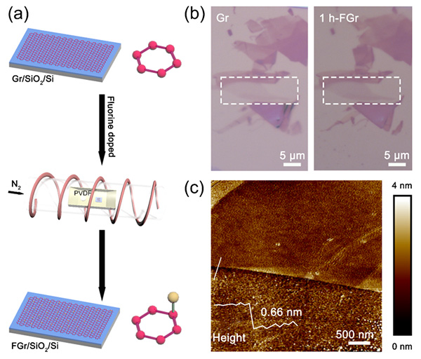
Characterization of the Gr and FGr. ©Yue Xue, Yaping Qi, Tong Tong, et al.
This work also connects to recent developments in van der Waals (vdW) heterostructures, which are created by layering different 2D materials to achieve multiple functions. Such structures have potential uses in memory storage, artificial intelligence, and photoelectric devices.
“The integration of fluorinated graphene into vdW heterostructures opens up exciting possibilities, especially for flexible electronics and systems that can perform multiple tasks at once,” stated Dr. Xichan Gao, a co-author and assistant professor at the Advanced Institute for Materials Research (AIMR) at Tohoku University.
“This research demonstrates how environmentally friendly processing can significantly improve the functional properties of graphene,” adds Qi. “Combining fluorination with strain engineering opens new possibilities for the development of scalable, high-performance 2D materials, providing a pathway to enhance graphene’s practical utility while maintaining a focus on safe and scalable material processing techniques.”
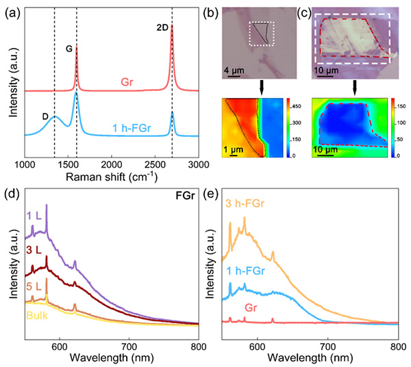
Raman and PL of the Gr and FGr. ©Yue Xue, Yaping Qi, Tong Tong, et al.
Details of the research were published in the journal Applied Physics Letters.
| タイトル: | Photoluminescence and transport properties of fluorinated graphene via a weak fluorination strategy |
|---|---|
| 著者: | Yue Xue, Yaping Qi, Tong Tong, Hang Xu, Zhenqi Liu, Cheng Ji, Jinlei Zhang, Ju Gao, Chunlan Ma and Yucheng Jiang |
| 掲載誌: | Applied Physics Letters |
| DOI: | 10.1063/5.0197942 |
| タイトル: | Van der Waals heterostructures for photoelectric, memory and neural network applications |
|---|---|
| 著者: | Hang Xu, Yue Xue, Zhenqi Liu, Qing Tang, Tianyi Wang, Xichan Gao, Yaping Qi, Yong P Chen, Chunlan Ma, Yucheng Jiang |
| 掲載誌: | Small Science (Selected for Cover) |
| DOI: | 10.1002/smsc.202300213 |
東北大学材料科学高等研究所(WPI-AIMR)
助教 Yaping Qi(研究者プロフィール)
| E-mail: | qi.yaping.a2@tohoku.ac.jp |
|---|
東北大学材料科学高等研究所(WPI-AIMR) 広報戦略室
| Tel: | 022-217-6146 |
|---|---|
| E-mail: | aimr-outreach@grp.tohoku.ac.jp |