06/28/2010

Microelectromechanical systems (MEMS) are miniature devices containing both electrical and mechanical components. The technology is an application of microfabrication for integrated circuits and draws together expertise in mechanics, optics and materials. “We call this heterogeneous integration,” says Masayoshi Esashi, a principal investigator at Tohoku University’s WPI-AIMR — he is also a global authority on MEMS technology. “By merging different technologies together, we can produce value-added MEMS devices with important core functionality in many systems.”
Esashi first encountered MEMS when he was an engineering student at Tohoku University in the early 1970s, and has spent the last 40 years working in the field. In his career, he has developed technologies for numerous MEMS devices that have become integral parts of our daily lives. Video game controllers, inkjet printers, digital cameras and automobiles are all examples of applications utilizing MEMS technology in some form or another.
“For example, a Nintendo Wii remote controller has a MEMS accelerometer that captures motion, which allows us to control the user interface and enjoy the game,” explains Esashi. “And one printer produced by Canon incorporates a MEMS print head with 6,000 nozzles for emitting small ink droplets, which allows it to print high-resolution images.”
Some of Esashi’s latest MEMS creations include an angular motion sensor developed in collaboration with Toyota researchers that detects any rotation of the car and compares it with the expected speed and angle of steering. When the sensor detects an unexpected spin situation, it automatically applies the brakes. Other transport-related applications for Esashi’s MEMS sensors included a two-dimensional optical scanner that is used in security surveillance equipment at Tokyo’s Haneda International Airport and at railway stations.
Advantest, the world’s largest semiconductor testing company, is also using Esashi’s MEMS switches in their latest large-scale integration (LSI) testers as a replacement for conventional switches based on electronic transistors, which are susceptible to electrostatic damage. The new MEMS switches are not affected by electrostatic discharge, making the LSI testers much more reliable. Elsewhere, the Japanese television channel NHK is using Esashi’s MEMS microphones in environments with particularly high humidity, such as in television studios for recording cooking programs.
Another important potential application for MEMS technology is in magnetic resonance imaging (MRI). “We have developed a thin cantilever holding an iron particle for detecting extremely weak magnetic resonance signals. It is used by the Japanese instrument maker JEOL,” explains Esashi. “They are using it for electron spin resonance imaging on micrometer-sized samples, which will enable the real-time visualization of the effects of medicine on cells.”
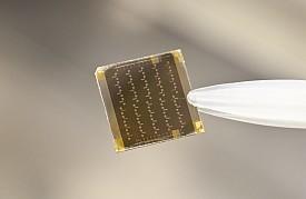
In addition to their small size, MEMS offer many advantages over conventional electromechanical devices. Esashi can make very small devices that provide extremely high sensitivity or spatial resolution, using extended microfabrication technology and at a fraction of the cost of conventional LSI devices.
“LSI fabrication typically involves the use of a photomask for transferring transistor patterns onto the silicon wafer. The mask can be very expensive, up to ¥500 million [US$5 million],” notes Esashi. “Therefore, such advanced technology is only viable for mass-production applications. For small-volume production, we are developing a MEMS-based maskless electron-beam exposure system, in which an electron beam is used to draw the transistor pattern on the wafer. The technology reduces costs and increases controllability, accuracy and versatility.”
Esashi believes that the future of MEMS lies in collaboration among academics and multiple commercial stakeholders — what he terms ‘company+company+university collaboration’ — and refocusing efforts on practical applications.
“We would like to support the industry by establishing a platform on which people can come together to work. We educate the researchers from companies. They learn, and then they go back to their companies to commercialize the technology, in many cases through inter-company collaboration. This is our way to contribute to society indirectly,” he says.
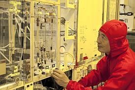
Esashi’s laboratory currently has 40 full-time researchers, including researchers from six companies of the likes of Fuji Film. His aim is to bridge the gap between pure research and application, while retaining the challenge and curiosity of scientific investigation. Within the WPI-AIMR, Esashi promotes joint research with the institute's bulk metallic glasses group on MEMS bonding technology with metallic glass and nanostructured metals.
“Our facilities are like toys. They are home-made instruments, giving researchers the chance for a fundamental experience not replicable in a company. If the researchers succeed in making devices using such equipment, they find it very rewarding and a lot of fun. This is very important for the researchers.”