07/30/2018
© 2018 Seigo Souma
Electrons in an ultrathin metal layer sometimes adopt the same behavior as electrons in the underlying substrate, AIMR researchers have found. Specifically, electrons in a two-atom-thick bismuth layer on tantalum sulfide (1T-TaS2) form a periodic formation known as charge density waves1. This finding offers a new way to control electrons in metal films and could have big implications for the application of topological materials to devices, such as field-effect transistors.
Interfaces between materials are of great interest to scientists because they often give rise to intriguing phenomena. In particular, a thin film on a substrate sometimes exhibits a property that the substrate possesses. For example, a metal film on a superconductor can become superconducting near the interface, and a nonmagnetic metal can become magnetic near its interface with a ferromagnetic material.
Now, Seigo Souma of the AIMR at Tohoku University and his co-workers have found that an analogous effect occurs for charge density waves — regular, wave-like arrangements of electrons that form in certain materials.
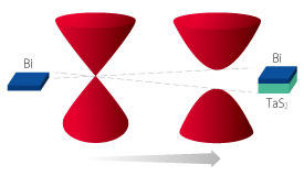
The researchers fabricated ultrathin films of bismuth on two substrates: silicon and 1T-TaS2 (charge density waves form in 1T-TaS2, but not in silicon). They then examined the electronic states in the bismuth films using spectroscopy and calculations.
The team discovered that electrons in the bismuth layer on silicon showed no departure from normal behavior; in other words, the substrate did not affect the bismuth. In contrast, they found that charge density waves formed in the bismuth layer on the 1T-TaS2 substrate. Moreover, this resulted in the formation of a gap in the energy levels of conduction and bound electrons (see image) within the bismuth.
This effect may offer electrical engineers a new way to manipulate electrons in metals. “Our results demonstrate that this effect can be used to tune the electronic band structure in a bismuth film,” explains Souma. “Since this effect opens up a relatively large energy gap, it will be useful for modifying the electronic states in films in contact with charge-density-wave materials. For example, this could be used to switch the energy gap in field-effect transistors.”
The team now intends to grow more complex compounds on 1T-TaS2. “We used bismuth in this study because it is a single element and relatively easy to grow,” says Souma. “Next, we will grow films of topological insulators and semimetals and study the effect on them. If it turns out that charge density waves can be used to tune the band gap of a topological insulator or semimetal, it will be an important breakthrough for the application of topological materials to devices.”
This research highlight has been approved by the authors of the original article and all information and data contained within has been provided by said authors.