04/28/2017
© 2017 Ziqian Wang
AIMR researchers have succeeded in measuring the three-dimensional structure of single layers of molybdenum disulfide (MoS2)1.
Two-dimensional materials are so called because they are single sheets of unit cells. While graphene is the two-dimensional material that has been grabbing the most headlines, its lack of a band gap limits its use in electronic applications. A class of materials known as transition-metal dichalcogenides (TMDs) shares some of the advantages of graphene but also has band gaps.
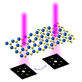
Now, Ziqian Wang, a graduate student of Mingwei Chen, of the AIMR at Tohoku University, and co-workers have shown for the first time that it is possible to glean three-dimensional information from a monolayer of the TMD molybdenum disulfide by using dynamic electron scattering. This technique allowed them to distinguish between two phases of the material: the semiconducting 1H phase and the metallic 1T phase. These two phases have different symmetries and can be transformed from one to another by ‘gliding’ a layer of sulfur atoms in MoS2.
Characterizing the three-dimensional structure of a two-dimensional material may seem like a contradiction in terms. But not all two-dimensional materials are perfectly flat—there is an intrinsic structure in the three-atomic-layer material so that some of their atoms lie above and beneath the plane of the sheet.
This intrinsic structure is important. “The three-dimensional structure may influence MoS2’s material properties as well as the properties of heterojunctions or stacking layers formed by combining MoS2 monolayers with other two-dimensional materials,” explains Wang. In the case of MoS2, the three-dimensional structure of the two-dimensional TMD material is critical for gaining a better understanding of the underlying mechanisms of the metal−semiconductor transition as well as for designing TMD electronic devices containing 1T−1H interfaces as metal−semiconductor conducts.
Images obtained by high-resolution electron microscopy techniques suppress this steric structure because they are basically two-dimensional projections of three-dimensional structures. In contrast, the dynamic scattering that occurs when an electron beam interacts with a monolayer sample encodes three-dimensional information in the resulting diffraction pattern. Thus, by comparing the intensities of diffraction spots within the pattern, researchers can recover information about the three-dimensional structure.
“Extracting three-dimensional information by analyzing electron diffraction patterns may compensate the weak points of transmission electron microscopy and scanning transmission electron microscopy imaging, especially for studying two-dimensional materials,” says Wang.
“This technique should also be applicable to other monolayer TMDs with the same phases and structures,” notes Wang. “And similar analyses of diffraction patterns should be useful for determining the three-dimensional structures of other two-dimensional materials.”
This research highlight has been approved by the authors of the original article and all information and data contained within has been provided by said authors.