
01/30/2017

Reproduced from Ref. 1 and licensed under CC BY 4.0 © 2016 N. H. Tu et al.
A junction that can be used to control currents flowing on the surfaces of a class of exciting new materials has been developed by AIMR researchers1. It promises to be useful for realizing compact, ultralow-power memory devices.
Exotic materials known as three-dimensional topological insulators are generating a lot of buzz among scientists because they could realize the revolutionary, power-saving technology of spintronics. Unlike electronics, which relies on the charge of electrons, spintronics mainly exploits a quantum property of electrons known as spin.
While the interior of a topological insulator is an electrical insulator, currents can freely flow on its surface with very low loss. But before these materials can be used for spintronics, researchers need to find ways to control the flow of current on their surfaces.
Elements known as p−n junctions are often used to control current in conventional electronic devices. They are so-called because they consist of two sections: one containing a dearth of electrons (the positive ‘p’ side) and the other containing an excess of electrons (the negative ‘n’ side). Currents can flow from the p to the n side, but not in the opposite direction.
However, conventional p−n junctions cannot be used to control current flow on the surfaces of topological insulators. Thus, the researchers needed to find a convenient way to switch currents on and off in these promising materials.
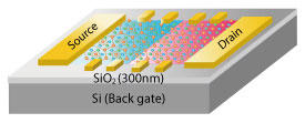
Katsumi Tanigaki, Yoichi Tanabe and their colleagues of the AIMR at Tohoku University fabricated their topological p–n junction on the surface of an ultrathin film of the topological insulator Bi1.5Sb0.5Te1.7Se1.3. They created the p side of the junction by adding a layer of an electron-accepting organic molecule to tune the chemical potential of the topological insulator.
But that by itself was not enough to form the junction. “Because the three-dimensional topological insulator has top and bottom surfaces, the chemical potentials of both surfaces have to be carefully controlled,” explains Tanabe, leader of the project in Tanigaki's group. The researchers achieved this by combining the organic molecule layer with a field-effect transistor technique.
When they did this, they observed a dramatic change in electrical transport on varying the gate voltage. Thus, the current flow could be controlled by simply varying the voltage applied to the junction.
The scientists are now working on optimizing their junction. “A very high gate voltage is needed to switch the topological p–n junction on and off,” says Tanabe. “We are trying to reduce the switching voltage by using different combinations of materials and organic molecules.”
This research highlight has been approved by the authors of the original article and all information and data contained within has been provided by said authors.