
04/25/2016

© 2016 Yuichi Ikuhara
By pinpointing the precise positions of atoms in titanium dioxide, AIMR researchers have studied how temperature and pressure affect the materials’ structure and properties1.
As their name implies, polycrystalline materials are made up of many small crystals. The interfaces between two of these small crystals are known as grain boundaries, the structure of which strongly affects material properties such as strength and electrical conductivity. Temperature or pressure changes can cause defects in a crystal’s atomic lattice to migrate to a grain boundary, which reshapes the structure of the boundary and hence modifies the material’s properties.
This process is extremely difficult to study because researchers need to see exactly where atoms sit relative to a grain boundary. While scanning transmission electron microscopy (STEM) can offer some insights, its usefulness is limited if the material contains low-mass atoms such as oxygen, which scatter electrons only weakly and hence are difficult to image by conventional STEM.
Now, Yuichi Ikuhara of the AIMR at Tohoku University and co-workers have applied two advanced STEM techniques — aberration-corrected high-angle annular dark-field (HAADF) STEM and annular bright-field (ABF) STEM — to study titanium dioxide, which is used in a wide range of applications, including catalysis, solar cells and gas sensors. The position of oxygen atoms in titanium dioxide’s grain boundaries can significantly affect the material’s conductivity and catalytic activity.
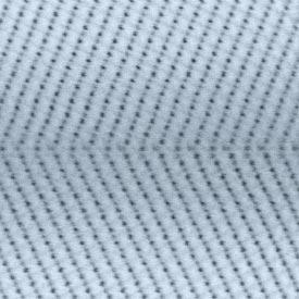
To simulate a grain boundary, the researchers bonded two crystals of titanium dioxide together (see image) and used HAADF and ABF STEM to reveal a neat line of oxygen atoms along the boundary.
When they heated these samples to 800 degrees Celsius under low pressure, the team found that some oxygen atoms were missing from the grain boundary. This should increase electrical conductivity along the boundary, says Ikuhara.
But heating the sample under a vacuum caused oxygen atoms to adopt a zigzag pattern along the grain boundary. “It is very surprising that these conditions could dramatically modify the atomic structure of grain boundaries in titanium dioxide,” says Ikuhara. When the researchers performed theoretical calculations to simulate these changes, they obtained good agreement with the experimental observations.
The results suggest that the properties of polycrystalline materials could be fine-tuned through heat or low-pressure treatments, optimizing them for use in electronic devices, for example. “We could control the grain boundary atomic structures to convert an insulating grain boundary into a conductive one,” suggests Ikuhara.
The team next plans to study how temperature and pressure affect the grain boundaries of other materials.
Sun, R., Wang, Z., Saito, M., Shibata, N. & Ikuhara, Y. Atomistic mechanisms of nonstoichiometry-induced twin boundary structural transformation in titanium dioxide. Nature Communications 6, 7120 (2015). | article
This research highlight has been approved by the authors of the original article and all information and data contained within has been provided by said authors.