
04/27/2015

© 2015 Chunlin Chen
Diamond and cubic boron nitride — the two hardest materials in the world — are vital components in abrasive cutting and polishing tools used in the manufacturing industry. Now, AIMR researchers have combined these two materials to create an interface that has radically different electronic properties from those of its constituents1.
The interfaces between two different materials are extensively used in applications as diverse as solar cells and magnetic recording devices. However, it is notoriously difficult to form interfaces between superhard materials because of the extreme rigidity of their lattices.
Chunlin Chen, Zhongchang Wang and Yuichi Ikuhara from the AIMR at Tohoku University, along with Takashi Taniguchi at the National Institute for Materials Science and collaborators in Japan, used the temperature gradient method to grow single crystals of cubic boron nitride on diamond seed crystals. They then explored the mechanism that allowed these two almost incompressible materials with extremely rigid lattices to join.
Lattice mismatch is a critical hurdle to achieving high-quality layer-by-layer crystal growth. It arises when parameters such as the bond lengths of the substrate and growth materials differ. Such mismatch induces strain in the crystal lattice, which can result in poor-quality films. While the difference between the bond length of cubic boron nitride (0.157 nanometers) and that of diamond (0.154 nanometers) is a minuscule 0.003 nanometers, it is large enough to cause growth complications in these extremely rigid materials.
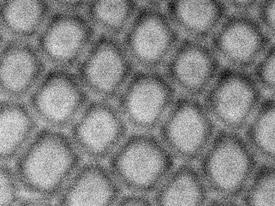
A frequently used method to overcome mismatch involves relieving lattice strain by introducing irregularities known as dislocations in the crystal lattice. Common forms of dislocations between two layers with different bond lengths are ‘misfit’ dislocations, where there are missing or dangling bonds between the two layers. Using atomic-resolution scanning transmission electron microscopy, Chen and Wang observed that the misfit dislocations in their system took the form of periodically arranged hexagonal loops connected by a continuous stacking fault network (see image). They discovered that the misfit accommodation mechanism differs remarkably from the conventional one.
“By combining transmission electron microscopy measurements with first-principles calculations, we confirmed that the carbon in diamond bonds directly to the boron in cubic boron nitride at the interface,” explain Chen and Wang, “and also that this bonding electronically induces a two-dimensional electron gas and a quasi-one-dimensional electrical conductivity, despite both bulk materials being insulators.”
Chen holds great hope for the new electronic states observed at the interface. “They could be manipulated for use in advanced electronic device applications, particularly those involving harsh conditions,” he says.
Chen, C., Wang, Z., Kato, T., Shibata, N., Taniguchi, T. & Ikuhara, Y. Misfit accommodation mechanism at the heterointerface between diamond and cubic boron nitride. Nature Communications 6, 6327 (2015). | article
This research highlight has been approved by the authors of the original article and all information and data contained within has been provided by said authors.