
12/22/2014

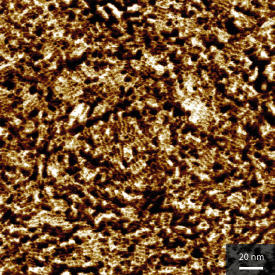
Modified, with permission, from Ref. 1 © 2014 American Chemical Society
An international team has captured unprecedented, three-dimensional (3D) images that reveal how polymers are organized in ‘bulk heterojunction’ (BHJ) organic solar cells1 — one of the most promising green devices for generating renewable electricity in an economically viable way. These new images can help settle long-standing debates on how molecules assemble at electrode interfaces, leading to improved manufacturing strategies.
The light-harvesting components of BHJ organic solar cells contain two materials that possess opposing electron-accepting and -donating abilities. To ensure efficient collection of solar energy, these materials must be blended until they are separated by no more than a few tens of nanometers. Most analytical techniques, however, can observe blended regions only in flat, two-dimensional planes, whereas actual devices are 3D.
Now, Dong Wang, Ken Nakajima and Thomas Russell from the AIMR at Tohoku University have used atomic force microscopy (AFM) to explore morphologies inside BHJ devices. AFM employs tiny needle-like probes to trace the topology of 3D surfaces, but it normally has trouble resolving polymer structures at molecular levels. The team overcame this limitation by using ultrasharp AFM tips that, as they are only a single nanometer wide, can image incredibly fine details on surfaces.
The researchers first prepared a standard BHJ device containing an aromatic electron-donor polymer known as PTB7 and a ‘buckyball’-like electron-acceptor material called PCBM. They then exposed the kinetically active working layers inside the BHJ by using high-energy argon ions to etch away the outer layers of the polymer blend.
Subsequent AFM, X-ray scattering and electron microscopy measurements revealed that the device’s active layer contained a continuous network of PTB7 fibrils, separated by tens of nanometers, interpenetrated by pathways of PCBM strands. This morphology changed at the electrode-contacting outer surface, where PTB7 crystals formed with PCBM aggregates embedded in-between (see image).
The researchers prepared devices containing different proportions of PTB7 and PCBM and discovered that the solar conversion efficiencies of these devices corresponded neatly to the length scales of the morphologies observed by AFM. According to Wang, this is clear evidence that three main factors — the PTB7 fibrils, the PCBM network, and the active mixing region — must be optimized to produce high-performance organic solar cells.
“These morphologies suggest that next-generation polymers need fibrils with fewer defects and better connectivity,” says Wang. “For the acceptor side, new materials that can form better and finer network domains will prove critical.”
Wang, D., Liu, F., Yagihashi, N., Nakaya, M., Ferdous, S., Liang, X., Muramatsu, A., Nakajima, K. & Russell, T. P. New insights into morphology of high performance BHJ photovoltaics revealed by high resolution AFM. Nano Letters 14, 5727–5732 (2014). | article
This research highlight has been approved by the authors of the original article and all information and data contained within has been provided by said authors.