07/28/2014
© 2014 WILEY-VCH Verlag GmbH & Co. KGaA, Weinheim
The perfect, honeycomb-like bonding inside a sheet of graphene allows charge carriers to move through the material as ‘massless’ particles called Dirac fermions. This phenomenon gives graphene intrinsically higher electron mobility than any other known material — a feature that promises to usher in an age of ultrafast and inexpensive carbon-based electronics. However, the atom-scale thinness that makes graphene so valuable also makes it difficult to manipulate into practical devices.
Yoshikazu Ito, Mingwei Chen and colleagues from the AIMR at Tohoku University have now discovered a way to produce three-dimensional (3D) nanoporous graphene structures that preserve the massless Dirac fermions — and thus the astonishing electron mobility — of two-dimensional (2D) systems1.
Turning graphene sheets into complex 3D networks is no easy task. A recently developed method, known as template-assisted growth, uses removable substrates to force carbon atoms into unconventional arrangements. This technique has successfully produced 3D graphene with intriguing mechanical and chemical properties. Yet the electrons inside these materials cannot travel efficiently because most templates have discontinuous or rough surfaces that introduce critical defects into the 3D framework.
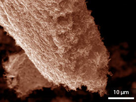
The researchers developed an improved template with a ‘bicontinuous’ structure containing a smooth, hard surface of nickel atoms and nanoscale pores. Then, by carefully heating this template in a chemical vapor deposition (CVD) chamber filled with hydrogen, argon and benzene gases, they grew uniform films of graphene all over the nickel template. Finally, they used acid to remove the nickel, yielding a freestanding, bicontinuous 3D structure of graphene and nanopores (see image).
Experiments revealed that the presence of the 3D nanopores, which the researchers could tailor by controlling the duration and temperature of the CVD process, had an enormous effect on graphene’s electron transport properties. The bicontinuous structure reduced the frequency of geometric defects that naturally appear when flat, hexagonally bonded sheets are formed into 3D shapes, thus helping to retain graphene’s 2D electronic character. 3D graphene with a large range of pore sizes behaved as high-speed quantum semiconductors, and the random orientations of the graphene sheets eliminated angular-dependent effects that often limit 3D device applications.
Ito explains that 3D nanoporous graphene has particular advantages over other graphene-based devices. “This material has abundant pore space for detecting molecules and promoting chemical reactions, in addition to its high charge mobility for applications in electronic devices,” he says. “We expect it could create a low-cost and ecofriendly alternative to gas sensors, transistors or energy-harvesting devices such as lithium–air batteries.”
Ito, Y., Tanabe, Y., Qiu, H.-J., Sugawara, K., Heguri, S., Tu, N. H., Huynh, K. K., Fujita, T., Takahashi, T., Tanigaki, K. & Chen. M. High-quality three-dimensional nanoporous graphene. Angewandte Chemie International Edition 53, 4822–4826 (2014). | article
This research highlight has been approved by the authors of the original article and all information and data contained within has been provided by said authors.