
06/30/2014

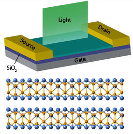
Modified, with permission, from Ref. 1 © 2014 American Chemical Society
Graphene — an ultrathin material consisting of a single layer of carbon atoms — has the potential to revolutionize electronic devices by making them smaller, faster and more efficient. One limitation of graphene, however, is that it can absorb only a small fraction of visible light. This prevents it from being used in photodetectors — optoelectronic components critical to the operation of solar cells and digital cameras.
Katsumi Tanigaki and colleagues from the AIMR at Tohoku University have now discovered a novel nanostructured material — gallium telluride (GaTe) flakes — that can detect light signals with a higher sensitivity and a faster electrical response than any existing two-dimensional (2D) layered material1.
Although electrons can move through the hexagonally bonded framework of graphene at extraordinary speeds, graphene’s ‘indirect’ optical bandgap means that any interaction with light must proceed via a time- and energy-consuming detour involving intermediate states. ‘Direct’ bandgap materials, in contrast, can absorb large quantities of photons by immediately converting them into a photoelectric current, making such materials extremely photosensitive.
The researchers’ extensive search for a direct-bandgap material that is atomically thin led them to GaTe crystals. This material’s unique structure — 2D sheets of Te–Ga–Ga–Te atoms (see image) stacked into weakly bonded, multilayered complexes — provides it with intriguing optoelectronic properties. Furthermore, GaTe is lightweight and easy to synthesize.
But when the researchers began their investigation, they encountered a crucial problem: the bandgap of GaTe changes from being direct to indirect when its bulk crystal structure is thinned down to a monolayer. Through collaborating with theoreticians from the United Kingdom to better understand the optical properties of this system, the team came to realize that finite, ten-layer GaTe stacks could yield the improved conductivity of 2D systems while retaining a direct bandgap.
To achieve this goal, the researchers resorted to a low-tech but effective method: using sticky Scotch tape to strip off very thin flakes from bulk GaTe crystals. This technique — pioneered for isolating single-layer graphene — produced the desired multilayered GaTe flakes, which they then transferred to a silicon device. Experiments showed that the tiny flakes could respond to a wide range of light within milliseconds. Importantly, the nanomaterials produced a photocurrent of light-generated electrons several orders of magnitude higher than that generated by graphene.
“A direct bandgap is very important for achieving both a high sensitivity and a fast response time in a photodetector,” says Tanigaki. “The intrinsic direct bandgap available from GaTe nanoflakes makes them a promising candidate for future photodetectors beyond graphene.”
Liu, F., Shimotani, H., Shang, H., Kanagasekaran, T., Zólyomi, V., Drummond, N., Fal’ko, V. I. & Tanigaki, K. High-sensitivity photodetectors based on multilayer GaTe flakes. ACS Nano 8, 752–760 (2014). | article
This research highlight has been approved by the authors of the original article and all information and data contained within has been provided by said authors.