
02/28/2011

Processing materials into thin films is important for fabricating electronic circuits, solar cells and lasers devices. Often only a few atomic layers thick, thin films are dominated by quantum effects whose properties can offer distinct performance advantages over thicker layers. Researchers from the WPI-AIMR in collaboration with researchers from Tsinghua University and the Institute of Physics in Beijing, China, have now uncovered how such quantum effects influence the properties of thin films based on the superconducting material lead1. Their findings could enable new electronic applications of thin metal films.
Thin films of lead are more unusual than those of most metals. Many of their properties are extremely sensitive to variations in film thickness, even by as little as a single atomic layer. This behaviour is thought to be caused by particularly pronounced quantum effects resulting from the long distances over which the electronic states of the metal extend, says Seigo Souma from the research team. “For most metals, quantum-size effects occur at very small thickness of less than 5 nm, whereas lead films, owing to their large electron wave length of 1 nm, exhibit significant size effects even at film thicknesses of over 20 nm.”
To discover the origins of these unusual quantum properties, the researchers studied thin films of lead grown on silicon. They combined two characterization techniques — surface scanning tunnelling spectroscopy and angle-resolved photoemission spectroscopy — to correlate the relationship between film thickness and any exhibited electronic features.
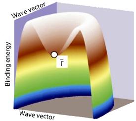
Charting the kinetic energy of the electrons as a function of their momentum, the researchers discovered that confinement effects caused the electronic states to form an ‘m’ shape (Fig. 1) that changes significantly between films comprising 23 and 24 atomic layers. Of particular interest is the circular structure that forms in the topmost part of the structure, where a very large number of electronic states are concentrated. The energetic position of the ring depends on the film thickness, which in turn causes thickness-dependent oscillations in the electronic properties of the films.
Building on this advancement in fundamental understanding, the next challenge will be to investigate the superconducting properties of these thin films together with systems of different geometries, such as quantum dots, wires and stripes. “Understanding the electronic structures of these low-dimensional systems lies at the heart of advanced electronic devices,” says Souma.
Sun, Y. J., Souma, S., Li, W. J., Sato, T., Zhu, X. G., Wang, G., Chen, X., Ma, X. C., Xue, Q. K., Jia, J. F., Takahashi, T. & Sakurai, T. Van Hove singularities as a result of quantum confinement: The origin of intriguing physical properties in Pb thin films. Nano Research 3, 800–806 (2010). | article
This research highlight has been approved by the authors of the original article and all information and data contained within has been provided by said authors.