01/31/2011
Thin oxide films are used in applications ranging from solar cells to transistors. They are made useful in part by the ability to tune many of their key properties, including conductivity and transparency. Some oxides can be changed from highly insulating to highly conductive by altering their structure or ‘doping’ them with foreign atoms. Zhongchang Wang and co-workers in the laboratories of Yuichi Ikuhara and Masashi Kawasaki at Tohoku University's WPI-AIMR in collaboration with researchers from the University of Tokyo and the Japan Fine Ceramics Center have now demonstrated a counter-intuitive way to induce an oxide to become conductive1.
The research team studied the conductivity of a thin film of a layered oxide composed of lanthanum, strontium and titanium. Using pulsed laser deposition, they were able to construct the film one atomic layer at a time with control over the nature of each layer. They focused on examining the effects of inserting insulating layers of SrTiO3 — a ceramic commonly used in electronic applications. Surprisingly, they found that the oxide underwent a transition from insulating to conductive behavior when a higher density of the insulating layers was included. This conductivity appeared without any change in the density of charge-carrying electrons, showing that the state was not the result of doping — a standard technique for raising conductivity.
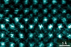
Wang and his colleagues investigated the effect of inserting the additional insulating layers using a combination of scanning electron microscopy (Fig. 1) and numerical simulations. Their studies showed that the addition of the insulating layers reduced distortion and bond strain in the oxide film. Distortion and strain can lead to insulating states by affecting the interactions between the electrons and the lattice, as well as the interactions among the electrons themselves. By allowing the material to relax to a less-strained state, the researchers were able to increase its conductance. Their data show that this counter-intuitive behavior arises from the creation of a conductive two-dimensional layer inside the oxide.
The results represent a new route to obtaining metallic behavior in materials that are normally expected to be insulators. The research team expects their finding to accelerate the search for superconducting and thermoelectric materials in oxides and other insulating materials. “Our first priority now is to consider whether superconductivity can be elicited in this particular oxide by reducing lattice disorder and structural defects so as to lower the barrier to charge carrier motion,” says Wang. The researchers believe that the material may also find use in high-mobility transistor and thermoelectric applications.
Wang, Z., Okude, M., Saito, M., Tsukimoto, S., Ohtomo, A., Tsukada, M., Kawasaki, M., Ikuhara, Y. Dimensionality-driven insulator–metal transition in A-site excess non-stoichiometric perovskites. Nature Communications 1, 106 (2010) | article
This research highlight has been approved by the authors of the original article and all information and data contained within has been provided by said authors.