09/28/2009
The composition and structure of the interfaces between crystallites in a polycrystalline material play an important role in determining the material’s properties and behavior. In electronic devices and microcomputer circuits, it is often the electronic properties of these interfaces, rather than those of the bulk materials, that form the basis for device operation. One way of controlling the characteristics of the interfaces is to add small amounts of impurities as ‘dopants’.
As the size of devices and material structures approaches nanometer scales, the influence of interfaces and dopant atoms becomes ever more significant. However, because dopant atoms are usually buried within the bulk material, it is difficult to obtain accurate information about their distribution at an interface, or the structure of the surrounding material. To address this issue, Yuichi Ikuhara from the Advanced Institute for Materials Research (AIMR) at Tohoku University and colleagues from the University of Tokyo1 have developed a technique that uses an electron microscope to image the location and local structure of individual dopant atoms within a buried interface.
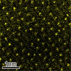
To demonstrate their approach, the researchers first doped an alumina surface with a low concentration of yttrium, which is known to strengthen the boundary between alumina crystals. This surface was then buried under a second alumina layer, added directly onto the first layer by diffusion bonding. The sample was subsequently imaged using a scanning transmission electron microscope — but in a slightly different way to how electron microscope images are usually taken.
Electron microscopy of crystalline materials is commonly carried out by directing an electron beam along one of the sample’s ‘strong channeling axes’ — particular directions in a crystal along which electrons can travel easily. This procedure usually improves the clarity of the images obtained, but can also conceal the presence of impurities. Instead, Ikuhara and his colleagues imaged their sample at an angle from these axes, which enabled them to obtain clear, high-contrast images of the yttrium atoms at the buried interface (see Fig. 1).
The ability to collect atomic-scale information about interfacial make-up and structure should enable researchers to better understand, and therefore better control, the doping of material interfaces. This in turn should help them to more easily engineer and optimize the properties of polycrystalline materials and the devices that rely on the behavior of the interfaces among crystallites.
Shibata, N., Findlay, S.D., Azuma, S, Mizoguchi, T., Yamamoto, T. & Ikuhara, Y. Atomic-scale imaging of individual dopant atoms in a buried interface. Nature Materials 8, 654–658 (2009). | article
This research highlight has been approved by the authors of the original article and all information and data contained within has been provided by said authors.