
~Development of spin-current thermoelectric conversion element with 100 times better performance in over 1 year~
NEC Corporation and Tohoku University applied new technologies developed by NEC, which use AI to predict the characteristics of unknown materials, to the joint development of cutting edge thermoelectric conversion technology known as a thermoelectric (TE) device*1 using spin current*2, and achieved 100 times better thermoelectric conversion efficiency over the course of approximately 1 year.
These new technologies consist of a group of AI technologies for material development which incorporate the various types of knowledge required for material development, and technology for the batch acquisition of the large amounts of material data that AI needs to learn material properties.
The AI technologies for material development use heterogeneous mixture learning technology*3 and a number of machine learning technologies specific to material development*4, *5 independently developed by NEC. These technologies were combined with technology for the batch acquisition of material data, which enabled the acquisition and evaluation of data regarding more than 1,000 types of materials with different compositions data and resulted in much more accurate AI learning.
NEC and Tohoku University applied a development technique combining these technologies to the development of a spin-current thermoelectric conversion device, and demonstrated that it is possible to enhance thermoelectric conversion efficiency by designing an actual material in line with AI-derived new material design guidelines.
In the future, NEC and Tohoku University will develop more sophisticated AI-based technologies for predicting the physical properties of new materials and conduct further research and development aimed at the practical application of spin-current thermoelectric conversion device technology and the realization of IoT devices that continue working for years without a power supply.
In recent years, cases in which machine learning technologies and analysis technologies based on informatics are applied to large amounts of data to extract hidden information and predict future trends are becoming increasingly common in a wide range of fields.
In the realm of natural sciences, there has long been research into the use of informatics in the search for new substances and materials and, especially in the biomedical, pharmaceutical and chemical fields, advances in so-called combinatorial technologies*6, which involve acquiring data through comprehensive investigation of search objects, have resulted in the extensive use of informatics in projects such as the human genome project.
Similarly, in fields that deal with solid state materials such as metals, semiconductors and oxides, techniques that make full use of the advantages of machine learning and analysis technologies from the viewpoint of shortening the duration of research and development and reducing costs are attracting attention in recent years as materials informatics (MI). Harnessing knowledge gained over many years of basic research in the natural sciences field using informatics, NEC began conducting research into analysis technologies specifically for solid state materials data more than five years ago. However, it was challenging because it took time and effort to produce and evaluate data in this field, making it difficult to obtain enough groups of data of sufficient quality required for the application of MI.
The initiatives of NEC and Tohoku University have now resulted in NEC’s independent development of AI technologies for material development that effectively analyze material data, and technology for the batch acquisition of data about many different types of solid state materials. NEC and Tohoku University have also applied a material development cycle incorporating these two types of technologies to the development of thermoelectric conversion materials using spin currents and considerably shortened the duration of material development.
1.Development of AI technologies for material development
A material development cycle using MI handles an enormous amount of material data and it is, therefore, inevitable that the data processing and classification and the data evaluation that was previously painstakingly performed by specialist researchers can no longer keep up. Also, in the development process, the amount of material candidates is generally greater than the amount of data that can be obtained, and selection of the process for searching these candidates needs to be performed more efficiently than in the past. To address these issues, NEC developed the following AI technologies for material development which correspond to the various characteristics of actual material data.
① AI technology for combinatorial data analysis: Machine learning technology for processing and classifying large amounts of data acquired using combinatorial techniques at high speed. Knowledge of physics/materials science is partially incorporated into existing machine learning algorithms to realize high precision, high speed data processing*4.
② AI technology for physical property modeling: Machine learning technology for evaluating large amounts of material data. Inductive modeling of physical properties using heterogeneous mixture learning with high readability (white-box) and high precision prediction enables researchers and AI to increase their understanding of data in concert. This technology plays a very important part in the extraction of the material parameter candidates that characterize the physical properties model.*3
③ AI technology for materials screening: Machine learning technology for efficiently searching for the target material from among a large amount of materials candidates. On the selection (screening) of materials with reference to the material parameters that characterize the physical properties model, the technology performs high-speed searches of ultra-multi-dimensional systems, which was difficult with existing Bayesian Optimization *7. This is achieved through the application of branch-and-bound type algorithm that predict moves into the future based on Combinatorial Game Theory. *5
2.Establishment of combinatorial data acquisition platform (batch evaluation and acquisition of large amounts of data)

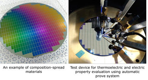
NEC and Tohoku University developed a combinatorial data acquisition platform that combines theoretical calculation data acquired through material property simulation with test data acquired through proprietary thin film materials preparation/characteristics evaluation technologies, to create enough data groups of sufficient quality.
In one example of composition-spread materials shown in the photograph, thin film material with more than 1,000 different types of composition was produced on a single substrate in one film preparation process. Electrode pads, etc. according to the purpose of measurement are patterned on the evaluation sample and experimental data can be acquired efficiently through an automatic evaluation system, which was also developed independently. The quality and amount of data is vastly improved compared to previous techniques used to produce and evaluate a single material in one experiment.
In the material physical property simulation, various calculation techniques are used according to the purpose, for example, first-principles calculations, and theoretical calculations are performed to ensure correspondence with experimental data. Various types of physical property parameter group, ranging from general physical properties such as electric resistance and thermal conductivity to detailed physical properties relating to electronic state are acquired as theoretical calculation data.
3.Application to the development of a spin-current thermoelectric conversion device
A spin-current thermoelectric conversion device recovers waste heat that exists widely in society by converting it into electricity and will, therefore, enable the countless IoT devices that will be installed in the future to continue working for many years even without a power source.
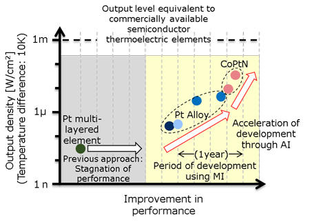
The main issue with a spin-current thermoelectric conversion device is that the thermoelectric conversion efficiency performance has still not reached a practically applicable level. When the recently established material development cycle combining a combinatorial data acquisition platform and AI technologies for materials development was applied on a trial basis to the search for a new platinum (Pt) alloy, this led to various discoveries, including that the Pt alloy was a magnet and the importance of the Pt itself contained in the alloy being spin polarized.

Evaluation of the characteristics of a new alloy CoPtN that is designed to enhance spin polarization of Pt according to AI-derived knowledge confirmed that thermoelectric conversion efficiency around 100 times higher than that of previous Pt alloy was obtained. This level was also much closer to the output level of commercially available thermoelectric conversion elements that use semiconductors. It was also demonstrated that it was possible to significantly shorten development time to around 1 year.

“We will continue to further expand the search for materials using AI in the future, focusing on further improvement in the thermoelectric conversion efficiency of spin-current thermoelectric conversion elements and the development of new low-cost materials.”, said Eiji Saitoh, Professor of Tohoku University. “We will also aim for the early practical application of spin-current thermoelectric conversion elements as power source technology for IoT devices that will continue to work for years without a battery or other power source and as low cost, high performance electronic cooling technology,” said Soichi Tsumura, General Manager, NEC IoT Devices Research Laboratories.
These results were achieved as part of the Exploratory Research for Advanced Technology (ERATO) “SAITOH Spin Quantum Rectification Project” (Research Director: Eiji Saitoh, Professor of Tohoku University; Research Period: 2014 - 2020 fiscal year) of the Japan Science and Technology Agency (JST) and the Promoting Individual Research to Nurture the Seeds of Future Innovation and Organizing Unique, Innovative Network (PRESTO) “Development of Basic Technologies for Advanced Materials Informatics through Comprehensive Integration among Theoretical, Experimental, Computational and Data-Centric Sciences” (Researcher: Yuma Iwasaki, NEC Corporation; Research Period: 2017 -2021 fiscal year) of JST.
NEC plans to exhibit and showcase these research findings at nano tech 2018 - The 17th International Nanotechnology Exhibition & Conference from February 14 (Wed) – 16 (Fri), 2018 at Tokyo Big Sight, Japan.
*1 A thermoelectric device is a device which converts thermal energy directly into electricity and vice versa.
*2 The spin current is a flow of a magnetic property of an electron, so-called “spin.”
*3 http://jpn.nec.com/ai/analyze/pattern.html
*4 “Comparison of dissimilarity measures for cluster analysis of X-ray diffraction data from combinatorial libraries” Y. Iwasaki et al., nature partner journal Computational Materials 3, 4 (2017).
*5 Proceedings of the 78th JSAP Autumn Meeting 5p-C18-4 (2017) R. Sawada et al.
*6 The combinatorial approach involves comprehensively investigating predicted combinations to gain an understanding of the overall trend of search candidates.
*7 Bayesian Optimization algorithms are stochastic optimization techniques that are used to search for the maximum or minimum value based on observed facts.