The quest for high throughput intelligent computing paradigms—for big data and artificial intelligence—and the ever-increasing volume of digital information has led to an intensified demand for high-speed and low-power consuming next-generation electronic devices. The “forgotten” world of antiferromagnets (AFM), a class of magnetic materials, offers promise in future electronic device development and complements present-day ferromagnet-based spintronic technologies (Fig. 1).
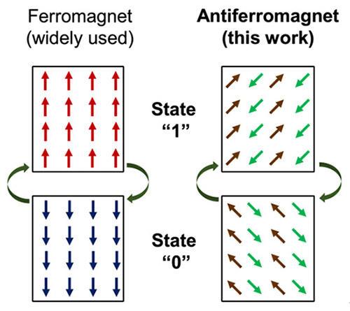
Figure 1: A schematic diagram of information storage using conventional ferromagnet (FM)-based spintronic devices (left) and the proposed antiferromagnets (AFMs)-based devices (right) (arrows indicate magnetic moments). In FM-based devices (left), bits of information (state “1” or “0”) is encoded in the orientation (red/up or blue/down) of the moments. The compensated structure of AFMs (right) entails unique advantages while posing significant hurdles at the same time.
Formidable challenges for AFM-based functional spintronic device development are high-speed electrical manipulation (recording), detection (retrieval), and ensuring the stability of the recorded information—all in a semiconductor industry-friendly material system.
Researchers at Tohoku University, University of New South Wales (Australia), ETH Zürich (Switzerland), and Diamond Light Source (United Kingdom) successfully demonstrated current-induced switching in a polycrystalline metallic antiferromagnetic heterostructure with high thermal stability.
The research group used a Mn-based metallic AFM (PtMn)/heavy metal (HM) heterostructure—attractive because of its significant antiferromagnetic anisotropy and its compatibility with PtMn Silicon-based electronics (Fig. 2(a)). Electrical recording of resistance states (1 or 0) was obtained through the spin-orbit interaction of the HM layer; a charge current in the adjacent HM resulted in spin-orbit torques acting on the AFM, leading to a change in the resistance level down to microsecond regime (Fig. 2(b)). “Interestingly, the switching degree is controllable by the strength of the current in the HM layer and shows long-term data retention capabilities,” said Samik DuttaGupta, corresponding author of the study (Fig. 2(c)). “The experimental results from electrical measurements were supplemented by a magnetic X-ray imaging, helping to clarify the reversible nature of switching dynamics localized within nm-sized AFM domains.” (Fig. 2(d),(e)).
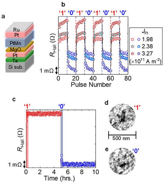
Figure 2: (a) A schematic diagram of the developed stack structure. (b) The experimental results of current-induced switching of AFM/HM PtMn/Pt structure under applied current JPt in the Pt layer. The reading of the antiferromagnetic states was achieved by measuring the output read resistance (RHall). (c) The stability of recorded states (1 or 0) was investigated by measuring RHall for several hours. Red and blue shaded area corresponds to the electrical recording of the high resistive (“1”) or low resistive (“0”) states. (d), (e) X-ray magnetic imaging of the PtMn/Pt structure after the application of current pulses. White and black areas of the image indicate regions of opposite magnetic contrast, representative of reversal of the antiferromagnetic order.
The results are the first demonstration of current-induced switching of an industry-compatible AFM down to the microsecond regime within the field of metallic antiferromagnetic spintronics. These findings are expected to initiate new avenues for research and encourage further investigations towards the realization of functional devices using metallic AFMs for information storage and processing technologies.
| Title: | Spin-orbit torque switching of an antiferromagnetic metallic heterostructure |
|---|---|
| Authors: | S. DuttaGupta, A. Kurenkov, O. A. Tretiakov, G. Krishnaswamy, G. Sala, V. Krizakova, F. Maccherozzi, S. S. Dhesi, P. Gambardella, S. Fukami and H. Ohno |
| Journal: | Nature Communications |
| DOI: | 10.1038/s41467-020-19511-4 |
Samik DuttaGupta
Center for Science and Innovation in Spintronics (CSIS), Tohoku University
| E-mail: | sdg@riec.tohoku.ac.jp |
|---|