A research group from Tohoku University led by current president Hideo Ohno has developed the world’s smallest (2.3 nm) high-performance magnetic tunnel junctions (MTJs). This work is expected to accelerate the advancement of ultrahigh-density, low-power, high-performance non-volatile memory for a variety of applications, such as IoT, AI, and automobiles.
The development of STT-MRAM—non-volatile spintronics memory—helps overcome the increasing power consumption in semiconductor device scaling. Crucial to integrating STT-MRAM in advanced integrated circuits is scaling magnetic tunnel junction—a core component of STT-MRAM—while improving its performance in data retention and write operation.
Shape-anisotropy MTJ, proposed by the same group in 2018, has shown MTJ scaling down to single-digit nanometers while achieving sufficient data-retention (thermal-stability) properties. In the shape-anisotropy MTJ, thermal stability is enhanced by making the ferromagnetic layer thick, Once the thickness goes beyond a certain point, however, device reliability becomes degraded.
To address the issue in the conventional shape-anisotropy MTJ with a single ferromagnetic structure [Fig. 1(a)], the group employed a new structure that uses magnetostatically coupled multilayered ferromagnets [Fig. 1(b)]. The developed MTJs were successfully scaled down to 2.3 nm in diameter— the world’s smallest MTJ size. They also exhibited high data retention properties up to 200°C and high-speed and low-voltage write operation down to 10 ns below 1 V at a single-digit-nanometer scale.
“The performance proves the developed MTJs’ capability to work with the future-generation advanced integrated circuits,” said Butsurin Jinnai, the first author of the study. “Because of its material compatibility with the standard MTJ material system, CoFeB/MgO, the proposed MTJ structure can be easily adopted in the existing MTJ technology.” The group believes that this will speed up the development of the ultrahigh-density, low-power, high-performance memory for a variety of applications, such as IoT, AI, and automobiles.
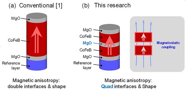
Figure 1: Schematic illustrations of the shape-anisotropy MTJ with (a) the conventional single ferromagnetic structure (developed in 2018) and (b) the multilayered ferromagnetic structure using magnetostatic coupling. In the multilayered ferromagnetic structure, device performance can be improved by enhancing the interfacial anisotropy, and two ferromagnets behave as a single magnet owing to magnetostatic coupling. This enables to make the ferromagnetic layer thinner while maintaining high thermal stability. [1] K. Watanabe et al., Nature Communications 9, 663 (2018).
| Title: | High-Performance Shape-Anisotropy Magnetic Tunnel Junctions down to 2.3 nm |
|---|---|
| Authors: | Butsurin Jinnai*, Junta Igarashi*, Kyota Watanabe, Takuya Funatsu, Hideo Sato, Shunsuke Fukami, and Hideo Ohno (*: equal contribution) |
| Conference: | IEEE International Electron Devices Meeting (IEDM) |
Shunsuke Fukami
Research Institute of Electrical Communication, Tohoku University
| E-mail: | s-fukami@riec.tohoku.ac.jp |
|---|