A research group from Tohoku University made up of Professor Hideo Ohno, Associate Professor Shunsuke Fukami, Associate Professor Hideo Sato, Assistant Professor Butsurin Jinnai, and Mr. Kyota Watanabe has revealed ultra-small magnetic tunnel junctions (MTJs) down to a single-digit-nanometer scale that have sufficient retention properties and yet can be switched by a current.
STT-MRAM (spin-transfer torque-magnetoresistive random access memory) has been intensively developed in recent years and commercialization by Mega fab companies is expected in 2018. The STT-MRAM is capable of replacing existing semiconductor-based working memories due to its excellent capabilities in terms of operation speed and read/write endurance. Moreover, it is nonvolatile, i.e., no power supply is required to retain stored information, making it indispensable for future ultralow-power integrated circuits.
MTJs are the heart of STT-MRAM. To continue the journey to increase the performance and capacity of STT-MRAM, it was essential to make the MTJ smaller, while maintaining the capabilities to retain information and be switched by a small current. CoFeB/MgO-based MTJs developed by the same group in 2010, in which an "interfacial anisotropy" at the CoFeB/MgO interface was utilized, paved the way down to around 20-nm generation. However, below 20-nm the desirable retention and switching properties could not have been realized simultaneously. Therefore yet another new approach was required.
The research group at Tohoku University used a "shape anisotropy", which had not been utilized effectively in devices suitable for integration, and developed ultra-small MTJs down to less than 10 nm, or a single-digit-nanometer scale.
The "shape-anisotropy" MTJ has a pillar-shaped magnetic layer, by which the film's normal direction becomes a magnetic easy axis due to the "shape anisotropy" (Fig. 1 (a)). This is in contrast to the "interfacial-anisotropy" MTJs, which were achieved by reducing the thickness of the magnetic layer (Fig. 1 (b)). The smallest diameter of MTJ studied was 3.8 nm, which is an unprecedented scale based on previous research endeavors.
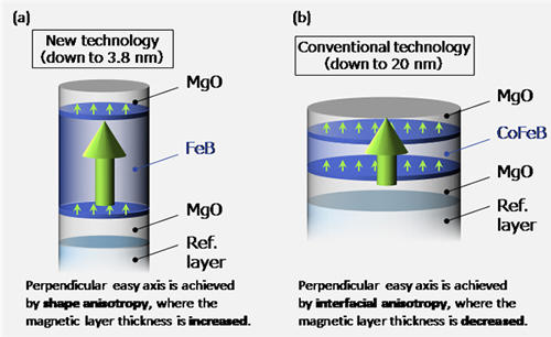 Fig. 1. Schematics for "shape-anisotropy" MTJ (a) and "interfacial-anisotropy" MTJ (b). The shape-anisotropy MTJ has a structure like a bar magnet standing.
Sufficiently high retention properties, represented by thermal stability factors, were obtained (Fig. 2); the obtained value of more than 80 had never been achieved through the conventional scheme. Furthermore, current-induced magnetization switching is observed for the "shape-anisotropy" MTJs with various diameters including below 10 nm devices (Fig. 3).
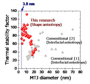 Fig. 2. Comparison of relation between thermal stability factor and MTJ diameter for the "shape-anisotropy" and "interfacial-anisotropy" MTJs. [1] S. Ikeda et al., Nature Materials 9, 721 (2010). [2] H. Sato et al., Applied Physics Letters 105, 062403 (2014).
The developed MTJ can work with generations of future semiconductor technologies. The single-digit-nanometer MTJ corresponds to more than 100 Giga-bit capacity, which is about 100-times larger than the current working memory technology.
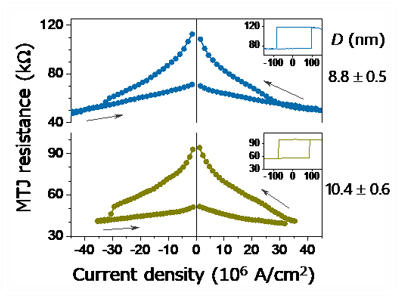
Fig. 3. MTJ resistance in response to applied current density for the fabricated "shape-anisotropy" MTJs with diameter D = 8.8 and 10.4 nm. Insets show the MTJ resistance as a function of out-of-plane magnetic field (unit: mT) for the same devices.
Authors: K. Watanabe, B. Jinnai, S. Fukami, H. Sato, and H. Ohno
Title: Shape anisotropy revisited in single-digit nanometer magnetic tunnel junctions
Journal: Nature Communications
DOI: 10.1038/s41467-018-03003-7
Shunsuke Fukami
Research Institute of Electrical Communication
Tohoku University
Email: s-fukami@riec.tohoku.ac.jp
Website: http://www.riec.tohoku.ac.jp/en/