07/29/2019
© 2019 Takafumi Sato
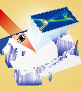
The mosaic surface of a multilayer structure made up of two materials with different topological properties has been imaged at a nanoscale resolution by AIMR researchers1. As well as providing important insights into the heterostructure, their results demonstrate the power of the nanoscale-resolution spectroscopy technique they used.
Exotic materials known as topological insulators have been attracting a lot of interest since their discovery a decade ago. Because of their topological properties, electric currents can flow on their surfaces but not inside them.
While blocks or thin films of topological insulators have been the main focus of research, structures made up of alternating layers of topological insulators and other materials are beginning to be explored. They have the advantage that their properties can be tuned by varying parameters like the thickness and stacking sequence of the layers.
“Such wide tunability is very useful for realizing novel topological phenomena,” notes Takafumi Sato of the AIMR at Tohoku University. “For example, inserting superconducting or magnetic layers into a crystal may realize topological superconductivity or the magnetoelectric effect, respectively.”
One useful technique for examining how the structural parameters of such multilayered structures affect the electrical properties of their surfaces is angle-resolved photoemission spectroscopy (ARPES). However, the beam of a conventional ARPES system is far too large to resolve the nanoscale variation in surface properties.
To overcome this, Sato and his co-workers at Tohoku University’s Department of Physics and elsewhere used a nano-ARPES system that has a beam size of about 120 nanometers — more than 800 times smaller than that of a conventional system — to probe the surface of a topological heterostructure made up of layers of lead selenide, a normal insulator alternating with layers of bismuth selenide, a topological insulator.
They were able to directly observe nanoscale domains on the surface of the heterostructure and determine their size, shape and distribution. Furthermore, the researchers could determine the electronic state of each domain and find out how the domains varied with the thickness of the topological insulator layers within a sample.
To conduct their experiments, the researchers traveled to France to use one of only about three nano-ARPES systems in the world. But in a few years they will be able to use a new synchrotron that is being constructed at Tohoku University.
And by using an even higher resolution nano-ARPES system, they hope to be able to resolve the boundary between different domains, which may host topological edge states that exhibit peculiar properties. “Nobody has ever observed this edge state directly by ARPES,” says Sato.
This research highlight has been approved by the authors of the original article and all information and data contained within has been provided by said authors.