09/25/2017
© 2017 Katsumi Tanigaki
A clever way of making thin films of exotic materials known as topological insulators has been developed by AIMR researchers1. It promises to overcome obstacles to the use of these emerging materials in electronic devices, including high-mobility transistors and thermoelectric devices for converting waste heat into useful electricity.
Topological insulators are generating much excitement among scientists because of their intriguing electrical and magnetic properties. In particular, they conduct electricity on their surfaces but are insulating in their interiors. This makes them suitable for use in the burgeoning area of spintronics, which is based on manipulating the spins of electrons rather than their charges. But to realize applications, a way is needed to produce large areas of high-quality three-dimensional topological insulators that are highly insulating in their interiors on a variety of substrates, including silicon.
Now, Katsumi Tanigaki and colleagues of the AIMR at Tohoku University have realized such a method for fabricating one of the most important topological insulators, Bi2−xSbxTe3−ySey (BSTS), on a wide range of surfaces. They first grew an ultrathin film of high-quality, single-crystal BSTS on a mica substrate using physical vapor deposition. The researchers then immersed the system in water, peeled the film from the mica and transferred it to other substrates.
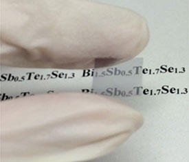
The transferred thin films exhibited excellent properties, including good electron and hole mobilities and spin chirality texture, indicating that they had not been damaged during transfer between substrates. Importantly, the researchers could produce large areas of BSTS films of about 1 square centimeter in size (see image). Furthermore, the fabrication method does not require a catalyst — a common source of impurities in other crystal-growth techniques.
“The most serious problem with three-dimensional topological materials has been that defects in their crystal structures have meant that their interiors are not perfectly insulating,” explains Tanigaki. “To achieve a pure topological surface, it is thus vital to minimize holes and electrons coming from the interior. Our thin-film crystal-growth technique realizes such an ideal situation.”
The ability to transfer films to different substrates is very useful. “Today’s electronic devices are fabricated almost exclusively by silicon-based technology. Our technique is a promising way to produce three-dimensional topological thin films on silicon substrates,” says Tanigaki. “Such thin films can also be transferred to transparent plastics for applications such as flexible wearable electronics.”
The researchers are exploring using the technique to produce thin films of other three-dimensional topological insulators. They are also looking at developing thermoelectric materials based on topological surface states, which could be used in devices that convert waste heat into electricity.
This research highlight has been approved by the authors of the original article and all information and data contained within has been provided by said authors.