
11/28/2016

© 2016 Yoichi Tanabe
Using their expertise for growing highly crystalline, three-dimensional (3D) graphene structures, AIMR researchers have produced a transistor with 1,000 times greater capacitance and conductance than transistors made from flat films of graphene1.
Electrons in graphene films have extraordinary mobility because they behave as particles with practically zero mass — so-called Dirac fermions. But graphene’s flat structure limits the number of electrons it can hold, making it challenging to incorporate graphene films in devices such as transistors.
One way to boost the capacitance of graphene-based devices is to assemble graphene films into porous nanoarchitectures that have large surface areas. However, it is tricky to preserve the high electron mobility of graphene in such 3D graphene ‘sponges’ because most fabrication methods introduce many defects, which retard or scatter charges.
Mingwei Chen from the AIMR at Tohoku University and colleagues recently developed a technique that overcomes this problem using nanoporous nickel templates. These hard metal surfaces enable the growth of ‘bicontinuous’ 3D graphene structures that bend and bond smoothly with few structural gaps.
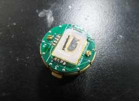
In their latest work, the AIMR team shows how to transform their 3D graphene structures into an electric double-layer transistor (EDLT) (see image). Unlike most transistors, the gates that control electron flow in EDLTs are made from nanometer-thin, capacitor-like charge layers that form at interfaces between an ionic liquid and a solid. The remarkably high accumulation of charges in the EDLT enables the electronic states of graphene to be controlled at very low operating voltages.
“This is one of the key devices needed to realize device applications with nanoporous graphene,” explains Yoichi Tanabe, a co-author of the study. “It allows us to control the number of carriers in the bicontinuous nanoporous material through the electric-field effect.”
After drying their 3D graphene structures under supercritical conditions to avoid damaging them, the researchers infused them with ionic liquid electrolytes and assembled the components into an EDLT. Using electrical measurements under a magnetic field, they developed a way to evaluate the nanoporous material’s mobility. They discovered that the advantageous properties of Dirac fermions remained. The device also offered exceptional electron switching behavior and conductance for further transistor applications.
“Being able to tune carrier densities means our nanoporous graphene EDLT can be a basis to design other electric devices. For example, high-response photodetectors could be developed in the future,” says Tanabe. “Also, diminishing the pore size in nanoporous graphene can introduce energy gaps into its electronic structure. Our EDLT technique could be one way to access these electronic states.”
This research highlight has been approved by the authors of the original article and all information and data contained within has been provided by said authors.