
12/21/2015

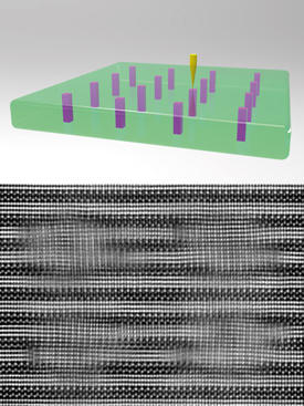
Adapted with permission from Ref. 1. Copyright 2015 American Chemical Society.
A way to switch the atomic packing of an inorganic crystal between two solid phases on a nanoscale has been developed by AIMR researchers led by Yuichi Ikuhara1. This technique, which uses a scanning transmission electron microscope (STEM) to produce patterns on a scale of mere nanometers, is promising for boosting the memory storage densities of computing devices.
Phase transformations in metallic crystals may be induced by applying a mechanical force or altering the temperature or pressure. These changes to the atomic structure often modify the properties of materials in beneficial ways, such as ‘shape-memory’ alloys that revert to their original forms on heating. However, triggering phase transformations on nanoscale dimensions to realize patterned devices is challenging because thermodynamic fluctuations make it difficult to precisely control atoms at such scales.
Recent advances in STEM imaging — particularly aberration-corrected lenses that produce subnanometer electron beams capable of resolving single atoms — have created new opportunities for controlling phase transformations on very small scales.
Now, Chunlin Chen and colleagues from the AIMR at Tohoku University, in collaboration with Johannes Georg Bednorz at IBM Research and researchers at ETH Zurich, have used a state-of-the-art STEM to study intriguing ceramics known as strontium niobates (SrNbOx). Slightly adjusting the oxygen content inside this material induces a transformation from layered atoms with insulating properties to a more compact ‘perovskite’ crystal packing with a high conductivity.
The team grew single crystals of SrNbOx and thinned them to microscale dimensions for STEM imaging. Initially, a layered structure appeared consisting of slabs of straight atomic chains alternating with slabs containing zigzag arrangements of atoms. Then, by increasing the STEM beam current for several minutes, the researchers squeezed oxygen atoms out of the crystal structure with an atom-by-atom accuracy. Images captured the phase transformation in action, showing the chain-like slabs zipping together to form the perovskite phase.
“It was exciting to see these images,” notes Chen, “because we realized this phase transformation could be used to fabricate nanodevices.”
To test this possibility, the team used the scanning STEM beam to create ‘nanopillars’: three-dimensional, elongated islands of the perovskite phase in a layered SrNbOx matrix (see image). The atomically sharp island boundaries and 5-nanometer interspacings they produced have the potential to realize higher storage densities in chips than modern memory devices, in which 20-nanometer separations are the norm.
The next challenge for the researchers is to fabricate the SrNbOx material in a thin-film device suitable for prototyping. They anticipate STEM-based phase transformations will have applications in material processing as well as next-generation nanodevices.
Chen, C., Wang, Z., Lichtenberg, F., Ikuhara, Y. & Bednorz, J. G. Patterning oxide nanopillars at the atomic scale by phase transformation. Nano Letters 15, 6469–6474 (2015). | article
This research highlight has been approved by the authors of the original article and all information and data contained within has been provided by said authors.