05/31/2010
© 2010 Z. Wang
The arrangement of atoms at the interface between a metal and a semiconductor plays a crucial role in determining the efficiency of electronic devices. But imaging atoms buried deep beneath the surface is not an easy task. Yuichi Ikuhara and co-workers from Tohoku University and Tokyo University1 have now produced an atomic-level picture of these technologically important interfaces by combining state-of-the-art imaging techniques and numerical simulations.
“Because we need to connect electrical components together using wires, a key issue that currently limits the efficiency of electronic circuits is the manufacture of reliable, low-resistance contacts between a metal and a semiconductor,” explains Zhongchang Wang, a member of the WPI-AIMR. A high-resistance barrier formed at some metal–semiconductor interfaces, known as a Schottky barrier, hinders the flow of electrons and increases power dissipation.
A good choice of metal and a process known as annealing — quickly heating to a high temperature — can overcome Schottky barriers. In the case of silicon carbide (SiC), a wide-bandgap semiconductor with potential applications in high-power and high-temperature applications, a trial-and-error approach has determined that titanium–aluminium (TiAl) alloys form such low-resistance contacts with SiC. “Researchers have suggested that a new metallic compound, Ti3SiC2, is formed between the deposited TiAl alloy and the SiC; however, it remained unclear how this interface could reduce the contact resistance.”
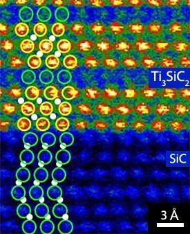
Ikuhara and his team deposited alternating layers of titanium and aluminium on a SiC substrate and then annealed them at 1000 °C for a few minutes. They produced an image of the precise arrangement of the atoms at the interface using a powerful technique known as Z-contrast scanning transmission electron microscopy (STEM), which is capable of distinguishing different atomic species. The titanium atoms appeared as bright spots whereas the silicon atoms were much darker (Fig. 1).
Numerical calculations simulated 96 possible interface geometries; only two of which matched the STEM image. In both of these variations, the silicon atoms in the metal (Ti3SiC2) sat in the spaces between silicon atoms in the semiconductor (SiC). In one case, however, carbon atoms, not visible in the STEM image because of their low mass, were also present at the interface (SiCSi). Further calculations indicated that this SiCSi arrangement was more stable than the other candidate (an SiSi interface) and that the presence of the carbon led to a much smaller Schottky barrier. “Our results suggest that an atomic layer of carbon plays an important role in reducing the contact resistance and provides a strategy for producing efficient SiC contacts,” says Wang.
Wang, Z., Saito, M., Tsukimoto, S. & Ikuhara, Y. Interface atomic-scale structure and its impact on quantum electron transport. Advanced Materials 21, 4966–4969 (2009). | article
This research highlight has been approved by the authors of the original article and all information and data contained within has been provided by said authors.