01/25/2010
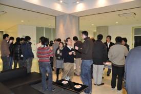
Every Friday evening, dozens of students, researchers and principal investigators flock into the lobby of the WPI-AIMR’s brand-new research building. Younger researchers especially look forward to the regular gathering as a great opportunity to mingle and chat freely with colleagues of any rank over coffee and cookies, where conversations can lead to new ideas and even joint projects.
The weekly ‘Tea Time’, a kind of informal event still unusual at Japanese research institutes and universities, is the latest example of an undertaking by the WPI-AIMR to provide young researchers with an unconstrained and stimulating environment to allow their potential to bloom. The WPI-AIMR’s endeavors have already begun to show fruit in the form of spontaneous and creative research activities, and more than 25 ‘fusion research’ projects have been created at the institute of 120 researchers since the first call for proposals was issued in March 2009. Fusion research is designed to encourage interdisciplinary interaction and collaboration among researchers with different backgrounds in an effort to spur synergies that could pave the way for new materials science.
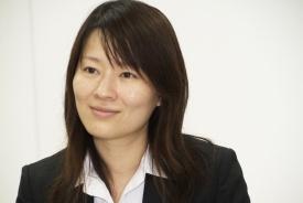
“Fusion research is one of the main reasons I came here,” says Yu-Ching Lin, an assistant professor of the Device/System Group specialized in micro-electromechanical systems (MEMSs). Before the WPI-AIMR was established, the Taiwanese researcher spent time at the Tohoku University School of Engineering, and later at the Fraunhofer Research Institution for Electronic Nano Systems in Chemnitz, Germany. Having studied practical and theoretical engineering, Lin reached a point where she felt the need to learn the basic materials science required to invent novel MEMS devices. Around that time, her supervisor, Thomas Gessner, director of the Fraunhofer ENAS who now concurrently serves as a principal investigator at the WPI-AIMR, recommended that she apply for her current position, and she jumped on the opportunity.
When Lin joined the WPI-AIMR in November 2008, she knew almost no-one. But the turning point arrived four months later when the WPI-AIMR held a week-long workshop. Lin had discussions with many researchers and found three eager collaborators from the Bulk Metallic Glasses Group—Na Chen, Deng Pan and Dmitri Louzguine. In April 2009, they submitted a proposal for a fusion research project and launched a project aimed at applying bulk metallic glasses (BMGs) for MEMS device fabrication.
MEMS devices are micrometer-sized sensors or actuators having electrical and mechanical elements mounted on a single board, and have origins in semiconductor technology with key emphases on materials, fabrication and device design. Historically, every introduction of an innovative material, such as polymers, silicon carbide, piezoelectrics and carbon nanotubes, has become a landmark event in the creation of a new realm of MEMS applications. “We believe now is the time for metallic glasses,” says Chen, a research associate, citing BMG’s unusual strength and formability.
When using conventional materials, lithography is employed to transfer patterns for MEMS devices. In addition to conventional fabrication techniques, however, the high formability and durability of metallic glasses could potentially allow such microscale parts to instead be cast using a mold, considerably simplifying the fabrication process. There is strong demand for a new MEMS fabrication scheme, but BMGs have been largely overlooked by engineers for use as MEMS parts. Lin’s team is now developing MEMS-compatible micro/nano fabrication methods for metallic glasses and investigating how to integrate BMG molding structures into MEMS devices.
But substantive technological challenges lie ahead, as metallic glasses have residual stress and poor adhesion to the silicon and silicon oxide used in complementary technologies. The team has tested a number of BMGs, and has found that parameters such as pressure and temperature are very important in the fabrication process. “By combining optimization of fabrication parameters and good selection of suitable BMG materials, we believe we can solve this bottleneck,” Lin says. Lin is also involved in another fusion research project formed by four principal investigators to examine the use of BMG as a novel bonding material for MEMS bonding technology. “Young people like me can be at the center of even ‘PI-level’ fusion research. That is really encouraging,” says Lin.
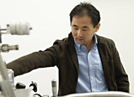
The WPI-AIMR philosophy has also attracted young Japanese scientists like Taro Hitosugi. When appointed as an associate professor of the Nanophysics Group, he was impressed with the institute’s generous support for the construction of an ideal laboratory at his own discretion. As a researcher of surface and interface physics, his work relies heavily on scanning tunneling microscopy (STM), which is extremely sensitive to noise and vibration. To shield his instruments from such interference, Hitosugi was allowed to cut out the laboratory floor, drill piles down into the bedrock, and pour 80 metric tons of concrete. The chamber is shielded with special double walls, each of which is 40 cm thick; but the combined effect is equivalent to 10 meters of concrete, says Hitosugi. “We have the best laboratory for STM in Japan, and the lab is one of the best in the world,” he says. “I’d like to take advantage of the WPI-AIMR as much as possible.”
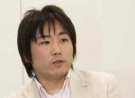
Like the weekly Tea Time, Hitosugi finds that fascinating projects are often conceived through casual interactions with Japanese and overseas colleagues. One day in 2009, Hitosugi dropped by the laboratory of Tadafumi Adschiri, principal investigator of the NanoChemBio Group and a specialist of novel nano-structural synthesis technologies. As their conversation developed from one topic to another, an idea for possible fusion research came up and Hitosugi was introduced to Daisuke Hojo, an assistant professor of the Adschiri laboratory.
One aspect of Hitosugi’s research is to produce nanoscale thin oxide films that show interesting physical properties such as superconductivity, and to investigate their electronic structures and functions at interfaces using STM. Hojo, on the other hand, synthesizes nanoparticles of metal oxides and bonds them with organic molecules in supercritical water. Usually, nanoparticles easily stick together, but Hojo’s synthesis allows nanoparticles to be dispersed uniformly in a solvent, making them easier to handle. These two researchers thought of combining their ‘dry’ and ‘wet’ processes to create innovative nanoparticles that acquire an anisotropic hetero-interface, which is impossible to achieve using wet processes only. “This is an unusual idea, but we can pursue maverick research here,” Hojo says. The new product could contribute to improve the properties of nanoparticles in applications such as semiconductors and catalysts, he adds.
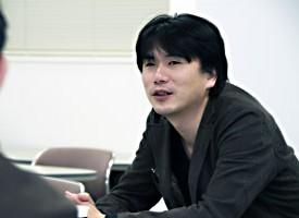
A different fusion research project is underway between Hitosugi and Shigemi Mizukami, an assistant professor specialized in spintronics—electronics utilizing the spin of electrons—in the Device/System Group. Their project is ambitiously aimed at changing the magnetic properties of a rechargeable battery by controlling lithium ions instead of electrons as in conventional systems. “I didn’t know ions behave so interestingly. We could change the paradigm of the battery system,” Mizukami says. The lithium-ion batteries in electric vehicles currently take about five hours to recharge. If the interaction between lithium-ion-diffusion and magnetism can be successfully controlled, however, lithium-ion batteries could be recharged much faster by applying a magnetic field to control the lithium ions.

The WPI-AIMR is not only generating spontaneous collaborations but also prompting young foreign talents to join the institute thanks in part to an incentive called the ‘Global Intellectual Incubation and Integration Laboratory Project’, dubbed ‘GI3’. Marco Haubold, a student of the Chemnitz University of Technology in Germany, spent five months at the WPI-AIMR to finish his diploma thesis. Like Lin, he primarily studied the theoretical aspects of MEMS materials, so he wanted to gain some experimental experience as well as discover the essence of interdisciplinary research. “After one month, I realized it would be very hard to take the responsibility for both theoretical and practical investigation,” Haubold says. “But that’s the challenge I wanted, and I am now feeling more competent.” Haubold returned to Germany in December, but another student Frank Roscher has recently arrived—also from Germany—with the intent of enhancing his breadth of vision to become a more able materials researcher. "In addition to the superb research environment at the WPI-AIMR, Sendai is a very comfortable place for research and living. Yes, I'd like to come back again," Haubold adds.