02/26/2018
© 2018 Chunlin Chen and Yuichi Ikuhara
By using transmission electron microscopy and first-principles calculations, a team of AIMR researchers has elucidated the origin of electron transport in a class of crystals that could be engineered to realize materials that conduct electricity in just two dimensions1. Such two-dimensional conductivity is promising for developing advanced electronic devices.
Solid oxides have been extensively studied by physicists and materials scientists alike because of the fascinating and useful properties that specific compounds can exhibit, including superconductivity, magnetism and ferroelectricity.
In particular, some oxide materials and structures exhibit electrical conductivity that is confined to two dimensions. One example is the family of compounds known as strontium niobates, which have the chemical formula SrnNbnO3n+2. Depending on the value of n, the members of this family can be conductors or insulators or exhibit quasi-one-dimensional conductivity (in other words, two-dimensional conductivity that is nearly confined along a line).
“Materials with two-dimensional conductivity have potential applications for novel electronic devices, such as metal–oxide–semiconductor field-effect transistors and transistors with high electron mobilities,” says Chunlin Chen, a researcher at the AIMR at Tohoku University.
To discover the cause of the unusual electrical behavior of SrnNbnO3n+2, a team led by Yuichi Ikuhara of the AIMR and Johannes Georg Bednorz of IBM Research - Zürich investigated the precise atomic and electronic configurations of various members of the family.
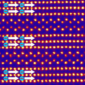
Scanning transmission electron microscopy revealed that each of these compounds consists of alternating stacks of zigzag-like and chain-like atomic slabs. The insulating or conductive behavior of the slabs depends on the valence of the niobium ions, which the team probed using a technique known as electron energy-loss spectroscopy. They discovered that zigzag-like slabs are insulating, whereas chain-like slabs are conducting.
Density functional theory calculations provided more insight into the origin of the insulating and conductive behaviors. Each slab has a backbone formed by NbO6 octahedra. The electrons associated with the atoms in these octahedra can move along the crystals, thus contributing to the conductivity. However, the team found that the octahedra in zigzag slabs are severely distorted, inducing a localization of the associated electrons and hence insulating behavior.
Aside from providing fundamental insights into the electrical properties of these materials, the results show that two-dimensional conductivity can be obtained by inserting insulating layers inside conductors. The AIMR team will attempt this experimentally. “We will try to confirm the concept of segmenting a three-dimensional conductor into a stack of quasi-two-dimensional conducting thin layers by inserting insulating layers in other materials,” says Chen.
This research highlight has been approved by the authors of the original article and all information and data contained within has been provided by said authors.