
10/28/2013

Reproduced, with permission, from Ref. 1 © 2013 American Chemical Society
Photodetectors, especially those that sense the infrared region of the electromagnetic spectrum, are important devices with uses in optical communication and imaging instruments. They rely on the generation of negative and positive charges — electrons and holes — by optical excitation. Subsequently, the charges are separated and contribute to an electrical current. However, in graphene, a material well known for its exceptional electronic properties and the foundation of several established photonics components, the electrons and holes rapidly recombine.
As a result, the amount of photocurrent that can be generated from a watt of incident radiation — the photoresponse — is very low, and preparing a graphene-based photodetector has remained a challenge. Now, Haixin Chang, Hongkai Wu, Mingwei Chen and Yuichi Ikuhara from the AIMR at Tohoku University and co-workers have demonstrated the possibility of enhancing the infrared photoresponse of graphene oxide, a close relative of graphene, by controlling the structure and number of defects in the material1.
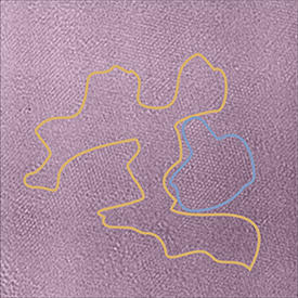
Chang’s team began by reducing few-layered graphene oxide through thermal annealing to improve its electronic properties. Then, they studied the structure and type of defects found in the original and reduced graphene oxide with transmission electron microscopy and X-ray photoelectron spectroscopy. While the original material contained large domains of highly ordered and disordered lattices (see image), thermal annealing decreased the size of both of these areas and also affected the nature of the oxygen-containing groups.
The researchers were able to directly link the structural modifications introduced during thermal annealing to changes in the few-layered graphene oxide’s photoresponse. Under infrared illumination, the team observed a photocurrent signal in the thermally annealed material that increased with the length of annealing — something they could not detect in the original.
Next, the team fabricated flexible infrared photodetectors from the reduced few-layered graphene oxide, finding the photoresponse of the devices to be over an order of magnitude higher than that of devices made from pristine graphene. The external quantum efficiency, a measure of the number of electrons and holes created by each photon under external bias, reached 97% — among the highest observed in graphene-based infrared photodetectors. Furthermore, the devices were very stable, retaining their photoresponse after 1,000 bending tests.
According to Chang, these findings could provide new ways to control the optoelectronic properties of graphene-based and other two-dimensional systems. His team is currently working to improve the response time of the reduced graphene oxide, which is still quite slow. “We believe that there are further opportunities to improve the photoresponse by further optimizing defects and atomic structures,” says Chang.
Chang, H., Sun, Z., Saito, M., Yuan, Q., Zhang, H., Li, J., Wang, Z., Fujita, T., Ding, F., Zheng, Z. et al. Regulating infrared photoresponses in reduced graphene oxide phototransistors by defect and atomic structure control. ACS Nano 7, 6310–6320 (2013). | article
This research highlight has been approved by the authors of the original article and all information and data contained within has been provided by said authors.